Product Description:
PCB Design is a PCB manufacturing and design service that specializes in Printed Circuit Board Design and Printed Circuit Board Design Service. Our PCB Design process is tailored to your exact specifications. We use high quality materials and components with a copper thickness of 1oz, test points, 2 layers, ENIG surface finish, and green solder mask color. Our PCB Design service is reliable and comprehensive, providing you with the best solution to your PCB needs.
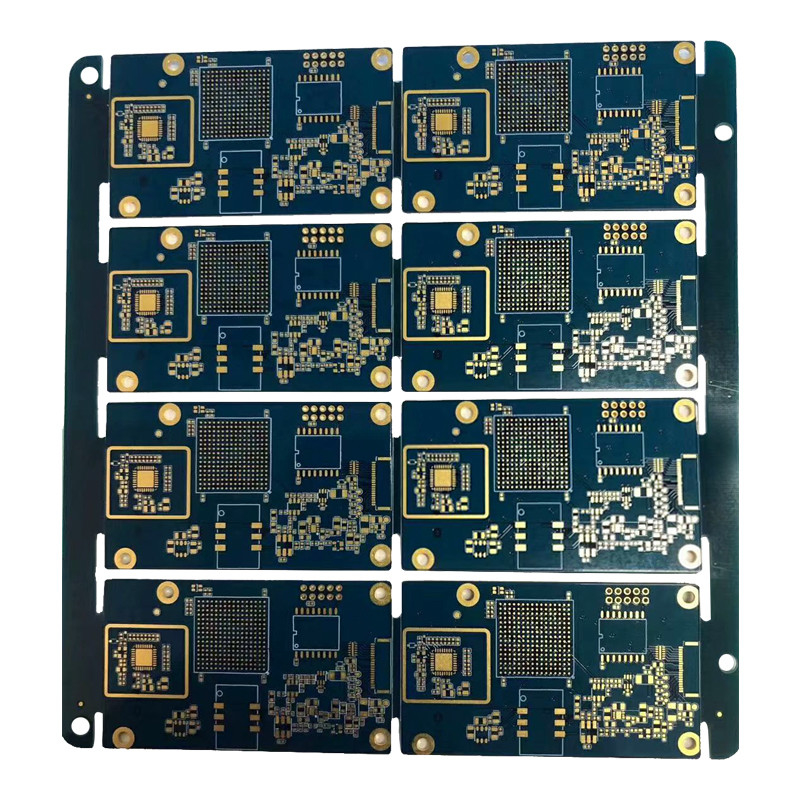
Features:
- Product Name: PCB Design
- Products type: AR, TV, AMD, DDR3, DDR4
- Silkscreen Color: White
- Test Points: Yes
- Minimum Trace Spacing: 6mil
- Layer Count: 2
- Electronic Circuit Design: Yes
- Electronics Printed Board Design: Yes
- Electronic Circuit Design and Fabrication: Yes
Technical Parameters:
| Description |
Specification |
| Silkscreen Color |
White |
| Minimum Annular Ring |
0.2mm |
| Board Size |
1200*610mm |
| Solder Mask Color |
Green |
| Minimum Trace Width |
6mil |
| Layer Count |
2 |
| Copper Thickness |
1oz |
| Surface Finish |
ENIG |
| Impedance Control |
Yes |
| Minimum Trace Spacing |
6mil |
Applications:
Hengxunda's Layout50012 is a high-precision circuit board fabrication designed for your most demanding applications. Featuring a white silkscreen color, green solder mask, 0.2mm minimum hole size, 6mil minimum trace width, and ENIG surface finish, this PCB fabrication design service is the perfect solution for a wide range of industries.
This advanced PCB design technology offers the highest levels of accuracy and reliability. The white silkscreen printing ensures easy reading of complex circuit board designs, while the green solder mask provides superior protection against moisture and oxidation. The 0.2mm minimum hole size ensures that your components are precisely fitted for optimal performance, and the 6mil minimum trace width ensures that your circuits are able to handle high current applications.
The ENIG surface finish offers superior corrosion protection and is ideal for high-frequency applications. Hengxunda's Layout50012 is ideal for use in automotive, aerospace, medical, telecommunications, and military applications. With its advanced PCB fabrication design services, you can be sure that your project is created with the highest level of precision and reliability.
Customization:
Customized PCB Design Service
Brand Name: Hengxunda
Model Number: Layout50012
Place of Origin: China
Silkscreen Color: White
Board Type: Multilayer Pcb
Layer Count: 2
Board Size: 1200*610mm
Minimum Trace Width: 6mil
We provide PCB Manufacturing Design and Circuit Board Fabrication service for your specific PCB design. Our experienced and professional engineering team will help you get the best PCB design to meet your exact specifications, including Brand Name, Model Number, Place of Origin, Silkscreen Color, Board Type, Layer Count, Board Size, Minimum Trace Width, etc.
Support and Services:
PCB Design Technical Support and Services
We provide technical support and services for PCB Design. Our team of experienced engineers is available to assist with any problems or questions you may have. Our services include:
- Assistance with PCB layout design
- Component selection and optimization
- Design for manufacturability (DFM) review
- Design verification and validation
- PCB fabrication and assembly
- Prototype testing and debugging
We strive to provide the highest quality of service and support for our customers. If you have any questions or need assistance with PCB Design, please contact us and we will be more than happy to help!
Packing and Shipping:
PCB Design Packaging and Shipping includes:
- Printed circuit board (PCB) is to be packaged in an antistatic bag.
- Additional components are to be packaged in separate antistatic bags.
- Final package is to be securely sealed using an appropriate sealant.
- Package is then to be shipped in a padded envelope to ensure safe delivery.
FAQ:
Q1: What is PCB Design?
A1: PCB Design is a process of designing an electronic circuit board for a product with the help of software, such as Hengxunda Layout50012.
Q2: What are the benefits of using Hengxunda Layout50012 for PCB Design?
A2: Hengxunda Layout50012 is a powerful PCB Design software with advanced features, such as automated design rule checking, advanced routing, 3D visualization and more. It also offers a wide range of components for designing PCBs.
Q3: Is PCB Design difficult?
A3: PCB Design is not an easy task but it can be made easier by using a reliable software like Hengxunda Layout50012. With the help of the software, you can easily design complex and reliable PCBs.
Q4: Where can I buy Hengxunda Layout50012?
A4: Hengxunda Layout50012 is available for purchase from various authorized resellers and distributors in China.
Q5: What is the difference between PCB Design and PCB Manufacturing?
A5: PCB Design is the process of designing the electronic circuit board with the help of software, such as Hengxunda Layout50012. PCB Manufacturing, on the other hand, is the physical creation of the circuit board by etching, drilling, and other processes.

 Your message must be between 20-3,000 characters!