Product Description:
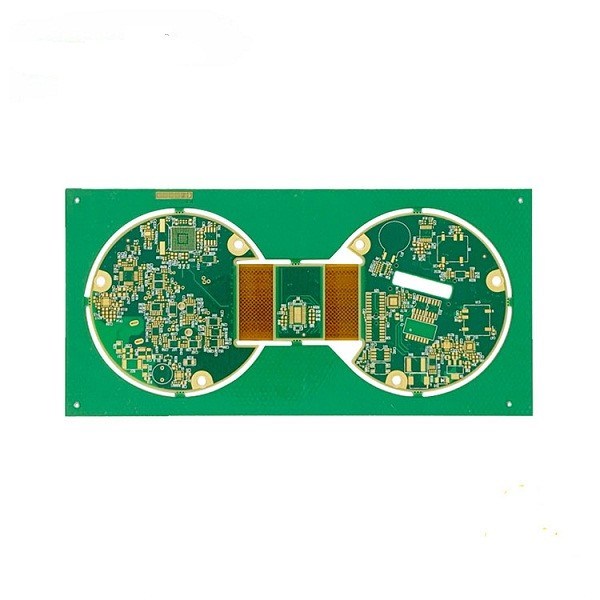
PCB Design is a type of printed circuit board fabrication and design, specialized in creating electrical circuits for a wide variety of products, including AR, TV, AMD, DDR3, and DDR4. It is a multilayer PCB with 2 layers, and the silkscreen color is white while the solder mask color is green. With its advanced electronics engineering services, PCB Design provides the most reliable and technically advanced electrical circuit design for all types of products. It offers great flexibility and accuracy in PCB design and fabrication, ensuring the highest quality of the printed circuit board. PCB Design is a great choice for customers who need to build a reliable and effective electrical circuit board for their products.
Features:
- Product Name: PCB Design
- Layer Count: 2
- Board Type: Multilayer Pcb
- Copper Thickness: 1oz
- Products type: AR, TV, AMD, DDR3, DDR4
- Board Size: 1200*610mm
- PCB Fabrication Design
- PCB Manufacturing Design
Technical Parameters:
| Parameter |
Value |
| Minimum Hole Size |
0.2mm |
| Board Type |
Multilayer Pcb |
| Impedance Control |
Yes |
| Test Points |
Yes |
| Material |
FR4 |
| Board Size |
1200*610mm |
| Minimum Trace Width |
6mil |
| Solder Mask Color |
Green |
| Minimum Trace Spacing |
6mil |
| Layer Count |
2 |
| Electrical Circuit Design |
Yes |
| PCB Manufacturing Design |
Yes |
| Electronic Circuit Design |
Yes |
Applications:
Hengxunda Layout50012 PCB Design is developed for the electronic circuit design industry. With its minimum trace spacing of 6mil, superior ENIG surface finish, white silkscreen color and impedance control technology, our PCB Design is the perfect choice for your circuit design needs. It also features test points for your convenience. Our PCB Design is developed with the latest technology to provide you with the best performance and accuracy. Make sure to choose Hengxunda Layout50012 PCB Design for all your Printed Circuit Board Pattern Design and Electronic Circuit Design needs.
Customization:
PCB Design Customization Services from Hengxunda
- Brand Name: Hengxunda
- Model Number: Layout50012
- Place of Origin: China
- Test Points: Yes
- Board Size: 1200*610mm
- Copper Thickness: 1oz
- Layer Count: 2
- Solder Mask Color: Green
- Services: PCB Fabrication Design, Electrical Circuit Design, Printed Circuit Board Design
Support and Services:
PCB Design Technical Support and Service
We provide technical support and services for PCB design. Our professional team of engineers are available to assist you with any questions you may have about your PCB design project. We can provide design advice, review your design, and answer any questions you may have about the design process.
We also provide services for prototyping and testing of your PCB designs. We can help you with testing and verification of your design to ensure the final product meets your requirements. We also provide training and support for CAD software and design tools used for PCB design.
Our team of experts have years of experience in the field of PCB design and can offer you the best advice and support for your project. We are committed to providing you with the highest quality of service and support. If you have any questions or need assistance with your PCB design project, please do not hesitate to contact us.
Packing and Shipping:
PCB Design product packaging and shipping includes the following steps:
- Check if all components of the PCB Design are packed correctly.
- Securely package the PCB Design product in a box or other appropriate container.
- Ship the packaged PCB Design product to the customer.
- Provide tracking information to the customer.
FAQ:
Q1: What is PCB Design?
A1: PCB Design is a board layout software from Hengxunda, with the model number Layout50012, which is made in China. It is a powerful tool for designing and creating printed circuit boards.
Q2: What are the main features of PCB Design?
A2: PCB Design offers a wide range of features, including: full-featured schematic and layout editors, advanced routing capabilities, real-time design rule checking, and support for a variety of manufacturing processes.
Q3: What types of files does PCB Design support?
A3: PCB Design supports a variety of file formats, including gerber, ODB++, DXF, and more.
Q4: What type of customer support is available for PCB Design?
A4: Hengxunda provides comprehensive customer support for PCB Design, including online tutorials, technical documentation, and customer service.
Q5: Does PCB Design offer any additional features?
A5: Yes, PCB Design offers a wide range of additional features, including: a powerful scripting language, advanced simulation capabilities, and support for a variety of manufacturing processes.

 Your message must be between 20-3,000 characters!