Product Description:
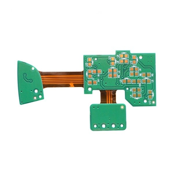
PCB Design is a comprehensive process that covers the entire process of PCB fabrication design, PCB layout design and PCB assembly. Our PCB Design services offer high-quality products with a minimum hole size of 0.2mm, surface finish of ENIG, multilayer PCB board type, minimum trace width of 6mil and silkscreen color of white. Our team of experienced professionals can help you with all aspects of PCB Design, from the early stages of design, to the final assembly of the PCBs. We use advanced technology to ensure that your PCBs are of the highest quality and provide you with the best value for money. We strive to make sure that our customers are satisfied with the results of their PCB Design process.
Features:
- Product Name: PCB Design
- Test Points: Yes
- Solder Mask Color: Green
- Board Type: Multilayer Pcb
- Material: FR4
- Surface Finish: ENIG
- Circuit Board Designing
- Circuit Board Fabrication
- PCB Fabrication Design
Technical Parameters:
| Parameter |
Value |
| Board Type |
Multilayer Pcb |
| Minimum Trace Width |
6 mil |
| Material |
FR4 |
| Impedance Control |
Yes |
| Minimum Hole Size |
0.2 mm |
| Copper Thickness |
1 oz |
| Silkscreen Color |
White |
| Minimum Annular Ring |
0.2 mm |
| Products Type |
AR, TV, AMD, DDR3, DDR4 |
| Layer Count |
2 |
| PCB Fabrication Design |
Yes |
| PCB Layout Design |
Yes |
| Printed Circuit Board Design |
Yes |
Applications:
Hengxunda's Layout50012 is the ideal PCB Design solution for electronic circuit design, electrical circuit design, PCB fabrication design and PCB layout design. It features a minimum hole size of 0.2mm, a board size of 1200*610mm, and impedance control and copper thickness of 1oz. Test points are also included for easy access and troubleshooting. With the highest quality standards, this PCB Design has been proven to be reliable and durable. Its superior features make it perfect for a wide range of applications, making it the perfect choice for all of your circuit board design needs.
Customization:
PCB Design – Hengxunda Layout50012
Hengxunda provides professional Electronics Printed Board Design, PCB Layout Design, and Electronics Printed Board Design Service to suit your precise requirements, including Brand Name: Hengxunda, Model Number: Layout50012, Place of Origin: china, Minimum Trace Width: 6mil, Surface Finish: ENIG, Layer Count: 2, Board Type: Multilayer Pcb, Minimum Annular Ring: 0.2mm.
Our experienced engineers ensure that all PCB Design products meet your requirements and offer a fast, reliable and cost-effective service.
Support and Services:
PCB Design Technical Support and Service
We provide technical support and service for PCB Design. Our support team is available 24/7 to answer any questions you may have regarding PCB Design. We can also provide custom solutions for PCB Design to meet your specific needs.
We also provide training and tutorials on PCB Design to help you get the most out of the product. This includes hands-on exercises, walkthroughs and online resources.
If you encounter any issues while using PCB Design, we are here to help. Please contact us at [email address] and we will be happy to assist you.
Packing and Shipping:
Packaging and Shipping
Packaging and shipping of PCB Design products is designed to ensure safe transport and storage of products. The steps for packaging and shipping include:
- Products are placed in protective bags.
- The products are then placed into a box or other shipping container.
- The box is then sealed with appropriate packing tape.
- The box is then labeled with the customer's address and other necessary information.
- The package is then shipped via the chosen shipping method.
FAQ:
Q1: What is the Brand Name of PCB Design?
A1: The Brand Name of PCB Design is Hengxunda.
Q2: What is the Model Number of PCB Design?
A2: The Model Number of PCB Design is Layout50012.
Q3: Where is PCB Design manufactured?
A3: PCB Design is manufactured in China.
Q4: Does PCB Design support custom specifications?
A4: Yes, PCB Design supports custom specifications.
Q5: Does PCB Design require professional installation?
A5: No, PCB Design does not require professional installation.

 Your message must be between 20-3,000 characters!