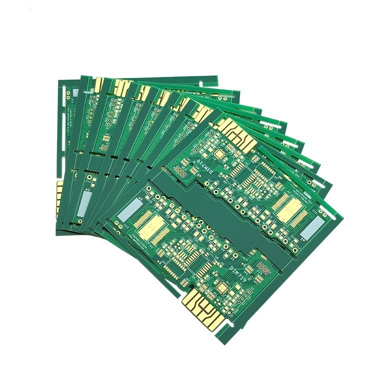
Product Description:
PCB Design is a highly specialized service for electronics printed board design. It offers a wide range of options for board layout design, from multilayer PCBs to single-sided boards. With its advanced trace width and annular ring technology, PCB Design ensures superior electrical performance, as well as impedance control, for a precise and reliable connection. Moreover, the board is finished with ENIG, which ensures surface finish quality and durability. PCB Design is the best choice for any electronics circuit board, providing quality, accuracy and reliability.
Features:
- Product Name: PCB Design
- Board Size: 1200*610mm
- Surface Finish: ENIG
- Products type: AR, TV, AMD, DDR3, DDR4
- Impedance Control: Yes
- Minimum Annular Ring: 0.2mm
- Electronics Printed Board Design: Yes
- PCB Pattern Design: Yes
- Circuit Board Designing: Yes
Technical Parameters:
| Parameter |
Value |
| Layer Count |
2 |
| Minimum Annular Ring |
0.2mm |
| Material |
FR4 |
| Board Size |
1200*610mm |
| Surface Finish |
ENIG |
| Impedance Control |
Yes |
| Products type |
AR, TV, AMD,DDR3,DDR4 |
| Copper Thickness |
1oz |
| Minimum Trace Spacing |
6mil |
| Solder Mask Color |
Green |
| PCB Fabrication Design |
Yes |
| PCB Pattern Design |
Yes |
Applications:
Hengxunda Layout50012 PCB Design is a multilayer printed board that is widely used in the electrical and electronic industry. It is designed to create complex electrical circuits and layouts with precise accuracy and minimum hole size of 0.2mm. The board is made of high quality FR4 material and finished with ENIG surface finish, which provides superior electrical performance and increased corrosion resistance. The copper thickness of 1oz ensures that the board can handle high current and voltage applications. This PCB design is used for a variety of applications such as automotive, aerospace, military, telecommunications, industrial automation, and consumer electronics. It is perfect for complex and precise electronics printed board design and electrical circuit designs.
Customization:
PCB Design - Customized Services from Hengxunda
Brand Name: Hengxunda
Model Number: Layout50012
Place of Origin: China
Material: FR4
Silkscreen Color: White
Minimum Annular Ring: 0.2mm
Minimum Trace Spacing: 6mil
Impedance Control: Yes
Hengxunda offers custom services in PCB Fabrication Design, Electronics Printed Board Design and PCB Manufacturing Design. Our PCB Design - Layout50012 is made of FR4 material and has a white silkscreen color. We provide a minimum annular ring of 0.2mm and minimum trace spacing of 6mil. Impedance control is also available.
Support and Services:
PCB Design Technical Support and Service
We offer comprehensive technical support and service for PCB design. Our team of experienced engineers and designers is available to answer any questions and help you throughout the entire design process. We provide:
- Design consultation to determine the best design for your application
- Design reviews to ensure proper design and functionality
- Design optimization to reduce cost and time to market
- Debugging and troubleshooting of existing designs
- Prototyping and fabrication services
- Product engineering and testing
- Design documentation and support
Our team is dedicated to providing you with the highest quality of service and support. For more information, please contact us.
Packing and Shipping:
Packaging and Shipping for PCB Design
The packaging and shipping process for PCB Design is simple and straightforward. To ensure the safety of the product during transit, the PCB Design product is first securely packaged in bubble wrap and then placed in a sturdy cardboard box. The box is then sealed with packing tape before being labeled with the necessary shipping information, including the address of the recipient. Once the package is ready, it is then picked up by the shipping carrier and transported to its destination.
FAQ:
- Q: What is PCB Design?
- A: PCB Design is a process of designing a printed circuit board (PCB) with Hengxunda's Layout50012.
- Q: What are the benefits of PCB Design?
- A: PCB Design helps to reduce the risk of product failure, improve reliability, and reduce the cost of the product.
- Q: What is the purpose of PCB Design?
- A: The purpose of PCB Design is to create a circuit board with the layout, components, and connections specified by the user.
- Q: What tools are used in PCB Design?
- A: The tools used in PCB Design include PCB design software, CAD software, and PCB layout software.
- Q: Where is Hengxunda’s Layout50012 PCB Design made?
- A: Hengxunda’s Layout50012 PCB Design is made in China.

 Your message must be between 20-3,000 characters!